There are three categories of materials based on their electrical properties:
(a) conductors
(b) semiconductors
(c) insulators.
The energy separation between the valence band and the conduction band is called Eg (band gap). The ability to fill the conduction band with electrons and the energy of the band gap determine whether a material is a conductor, a semiconductor or an insulator.
Electrons in solids materials
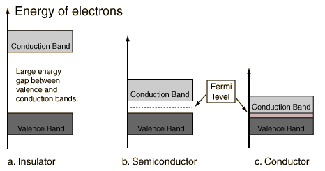
Insulators
Core shell electrons are tightly bound to atoms, and do not interact strongly with electrons in other atoms, Valence shell electrons are the outer electrons that contribute to bonds between atoms core valence conduction Electron energy. If all of the bonds are “satisfied” by valence electrons, and if these bonds are strong, then the material does not conduct electricity. Insulators have large bandgaps that require an enormous amount of voltage to overcome the threshold. This is why these materials do not conduct electricity.
Semiconductors
If all the bonds are “satisfied”, but the bonds are relatively weak, then the material is an intrinsic semiconductor, and thermal energy can break a small number of bonds, releasing the electrons to conduct electricity. Electronic configuration in an intrinsic semiconductor If impurities with one more or one fewer electrons than a host atom are substituted for host atoms in a semiconductor, then the material becomes conductive - an extrinsic semiconductor. Electronic configuration in an extrinsic semiconductor, in semiconductors, the band gap is a few electron volts. If an applied voltage exceeds the band gap energy, electrons jump from the valence band to the conduction band, thereby forming electron-hole pairs called exactions.
Conducting materials
If only a fraction of the bonds are satisfied (or alternatively, if there are many more electrons than are needed for bonding) then there is a high density of electrons that contribute to conduction, and the solid is a metal. Electronic configuration in conducting materials in conducting materials like metals, the valence band and the conducting band overlap, so the value of Eg is small: thermal energy is enough to stimulate electrons to move to the conduction band. If only a fraction of the bonds are satisfied (or alternatively, if there are many more electrons than are needed for bonding) then there is a high density of electrons that contribute to conduction, and the solid is a metal.
Quantum confinement and its effect on material Electronic properties
In Nano crystals, the electron energy levels are not continuous as in the bulk but are discrete (finite density of states) because of the confinement of the electron wave function to the physically dimensions of the particles. This phenomenon is called Quantum confinement and therefore Nano crystals are also referred to Quantum dots. Quantum confinement causes the energy of the band gap to increase. Furthermore, at very small dimensions when the energy levels are quantified, the band overlap present in metals disappears and is actually transformed into a band gap. This explains why some metals become semiconductors as their size
is decreased.
The increase in band gap energy due to quantum confinement means that more energy will be needed in order to be absorbed by the band gap of the material. Higher energy means shorter wavelength (blue shift). The same applies to the wavelength of the fluorescent light emitted from the nano-sized material, which will be higher, so the same blue shift will occur. Thus, a method of tuning the optical absorption and emission properties of a nano-sized semiconductor over a range of wavelengths by controlling its crystallite size is provided. The optical properties of nano-sized metals and semiconductors (quantum dots). Nanomaterials with exceptional electrical properties Some nanomaterials exhibit electrical properties that are absolutely exceptional. Their electrical properties are related to their unique structure. Two of these are fullerenes and carbon nanotubes. For instance, carbon nanotubes can be conductors or semiconductors depending on their nanostructure. Another example is that of supercapacitors materials in which there is effectively no resistance and which do not obey Ohm’s law.
Size effect in metal and semiconductor
In any material, there will be a size below which there is substantial variation of fundamental electrical and optical properties with size, when energy level spacing exceeds the temperature. For a given temperature, this occurs at a very large size (in nanometers) in semiconductors as compared with metals and insulators. The quantum size effect is most pronounced for semiconductor nanoparticles, where the band gap increases with a decreasing size, resulting in the interband transition shifting to higher frequencies.
Effects of Nano size in electrical properties
Properties depends on size, composition and structure:
• Nano size increases the surface area
• Change in surface energy (higher)
• Change in the electronic properties
• Change in optical band gap
• Change in electrical conductivity
• Higher and specific catalytic activity
• Change thermal and mechanical stabilities
• Different melting and phase transition temperatures
• Change in catalytic and chemical reactivities
Electronics
Electronics is the science of how to control electric energy, energy in which the electrons have a fundamental role. Electronics deals with electrical circuits that involve active electrical components such as vacuum tubes, transistors, diodes and integrated circuits, and associated passive electrical components and interconnection technologies. Commonly, electronic devices contain circuitry consisting primarily or exclusively of active semiconductors supplemented with passive elements; such a circuit is described as an electronic circuit. The nonlinear behaviour of active components and their ability to control electron flows makes amplification of weak signals possible, and electronics is widely used in information processing, telecommunication, and signal processing. The ability of electronic devices to act as switches makes digital information processing possible. Interconnection technologies such as circuit boards, electronics packaging technology, and other varied forms of communication infrastructure complete circuit functionality and transform the mixed components into a regular working system.
Electronics is distinct from electrical and electro-mechanical science and technology, which deal with the generation, distribution, switching, storage, and conversion of electrical energy to and from other energy forms using wires, motors, generators, batteries, switches, relays, transformers, resistors, and other passive components. This distinction started around 1906 with the invention by Lee De Forest of the triode, which made electrical amplification of weak radio signals and audio signals possible with a non-mechanical device. Until 1950 this field was called "radio technology" because its principal application was the design and theory of radio transmitters, receivers, and vacuum tubes. Today, most electronic devices use semiconductor components to perform electron control. The study of semiconductor devices and related technology is considered a branch of solid-state physics, whereas the design and construction of electronic circuits to solve practical problems come under electronics engineering.
Nanoelectronics
Nanoelectronics are part of the nanotechnology domain, which deals with the characterization, manipulation and fabrication of the electronic devices at the nanoscale. Nanoelectronics is one of the major technologies of Nanotechnology. It plays vital role in the field of engineering and electronics. Nanoelectronics make use of scientific methods at atomic scale for developing the Nano machines. The main target is to reduce the size, risk factor and surface areas of the materials and molecules. Machines under nano electronic process undergoes the long range of manufacturing steps each with accurate molecular treatment. This article focuses on engineering aspects of Nanoelectronics.
The Nanotechnology field has been the subject of intense focus, particularly from the viewpoint of the electronics industry. The commitment is, no doubt, driven to a large measure by the current top-down methodologies for fabrication of silicon- based devices. This is implied in the next-generation approach towards manufacture of MEMS, microprocessors, optical switching and several other electronic components. Nanoelectronic devices; are a very small devices to overcome limits on scalability.
Nanotechnology is continually playing vital role to improve the capability of electronic products. The technology also made the devices very light making the product easy to carry or move and at the same time it has reduced the power requirement. Some Consumer Products which are using Nanotechnology:
- Computer Hardware
- Display Devices
- Mobile & Communication Products
- Audio Products
- Camera & Films
- The world market for nanoelectronics is expected to reach $409.6 billion by 2017.
Nanoelectronic configuration
The electronic configurations of Nanomaterials are significantly different from that of their bulk counterpart. These changes arise through systematic transformations in the density of electronic energy levels (Density of states (DOS)) as a function of the size, and these changes result in strong variations in the optical and electrical. While the DOS in a band could be very large for some materials, it may not be uniform. It approaches zero at the band boundaries, and is generally higher near the middle of a band. The density of states for the free electron model. In statistical and condensed matter physics, the density of states (DOS) of a system describes the number of states at each energy level that are available to be occupied. A high DOS at a specific energy level means that there are many states available for occupation. A DOS of zero - no states can be occupied at that energy level. near the middle of a band. The density of states for the free electron model in three dimensions is shown by figure.

Importance of Nanostructures in Electronic
Nanotechnology is already being used by the electronic industry and you will be surprised to know that many of today’s electronics have already incorporated many applications that the nanotechnology science has developed. For example, new computer microprocessors have less than 100 nanometers (nm) features. Smaller sizes mean a significant increase in speed and more processing capability.
These advances will undoubtedly help achieve better computers. However, at some point in time (very near in the future) current electronic technology will no longer be enough to handle the demand for new chips microprocessors. Right now, the method for chip manufacturing is known as lithography or etching. By this
technology, a probe literally writes over a surface the chip circuit. This way of building circuits in electronic chips has a limitation of around 22 nanometers (most advanced chip processors uses 60-70 nm size features). Below 22 nm errors will occur and short circuits and silicon limitations will prevent chip manufacturing.
The Electronic behavior of Materials at Nanoscale
Materials behave electronic differently at Nanoscale for two reasons: Firstly, very small particles have a larger surface area compared to the same amount of material in a larger lump (for example, grains of sand would cover a bigger surface than the same amount of sand compressed into a stone). As the surface of the particle is involved in chemical reactions, the larger surface area can make materials more reactive – grains of salt dissolve in water much more quickly than a rock of salt for example. In fact, some materials that are generally inactive in their larger form can be more reactive in nanoscale. Secondly, when we look at materials on a nanoscale level, the relative importance of the different laws of physics shift and effects that we normally do not notice (such as quantum effects) become more significant, especially for sizes less than 20nm.
This is mainly due to the nanometer size of the materials which render them:
1. large fraction of surface atoms;
2. high surface energy;
3. spatial confinement;
4. reduced imperfections
ELECTRONS NANOSTRUCTURES APPLICATION
Nanoelectronics refer to the use of nanotechnology in electronic components. the section covers a diverse set of devices and materials, with the common characteristic that they are so small that inter-atomic interactions and quantum mechanical properties need to be used extensively. Some of these include: hybrid molecular/semiconductor electronics, one-dimensional nanotubes/nanowires, or advanced molecular electronics. Recent silicon CMOS technology generations, such as the 22 nanometernode, are already within this regime. Nanoelectronics are sometimes considered as disruptive technology due to the significantly different from traditional transistors.
Nanoelectronic Devices
Nanotechnology Makes many Nanoelectronic digital Devices such as:
• Nano Transistors
• Nano Memory
• Nano Circuitry
• Nano Diodes
• OLED (Organic Light Emitting Diode)
• Plasma Displays
• Quantum Computers
• Nano sensors
• Nano rods
• I pods
• Nanogears
No comments:
Post a Comment